NXP Semiconductors FS6500 System Basis Chip
NXP Semiconductors FS6500 System Basis Chip (SBC) is a multi-output, SMARTMOS Power Supply Integrated Circuit (PMIC), featuring CAN FD (Controller Area Network Flexible Data) and/or LIN (Local Interconnect Network) transceivers. NXP FS6500 SBC provides power to MCUs and optimizes energy consumption through DC-DC switching regulators, linear regulators, and ultra-low-power-saving modes.The FS6500 SBC includes configurable fail-safe/fail silent safety behavior and features, with two fail-safe outputs, becoming a full part of a safety oriented system partitioning, to reach a high integrity safety level (up to ASIL D). Multiple switching and linear voltage regulators, including a 32μA low-power mode, are available with various wake-up capabilities. An advanced power management scheme is implemented to maintain high efficiency over a wide range of input voltages down to 2.7V, and output current ranges up to 2.2A.
The built-in CAN FD interface fulfills the ISO 11898-2 (12) and -5(13) standards. The LIN interface fulfills LIN protocol specifications 2.0, 2.1(22), 2.2(23), and SAE J2602-2(24).
The FS6500/FS4500 feature configurable fail-safe/fail silent safety behavior, with two fail-safe outputs, becoming a full part of a safety-oriented system partitioning, to reach a high integrity safety level (up to ASIL B).
High-temperature capability up to TA = 125°C and TJ = 150°C, compliant with AECQ100 Grade 1 automotive qualification.
Features
- 2.7V up to 28V voltage operation range
- Buck pre-regulator with optional boost to fit with LV124 automotive test standards
- Ultra-low 30µA power modes
- Multiple wake-up sources in low-power mode: CAN, LIN, I/Os, LDT
- 3.3V keep alive memory supply available in low-power mode
- Independent fail-safe state machine supporting high functional safety standards
- Robust physical layers with superior EMI/ESD performance
- Five configurable I/Os
- 0.5A to 2.2A dual DC-DC supply
- Fail silent configurable safety architecture allowing independent monitoring of critical parameters and system availability
- System integration: analog multiplexer, battery sensing, long duration timer, and live memory supply to reduce BOM
- Scalable family, with a large range of pin-to-pin compatible part numbers supporting different system configurations for design flexibility
- Meets grade 0 reliability performance levels: qualified with 1300 hours of HTOL stress at Tj=+175°C
- 7mm x 7mm, 48-pin LQFP package, 0.5mm pitch
Applications
- Electric vehicles
- Hybrid electric vehicles
- Battery management systems
- Safety-critical motor control
- ADAS (advanced driver-assistance systems)
- Forward collision warning (FCW)
- Lane departure warning (LDW)
- Radar
- Sensor fusion safety area
- Drive train electrification
- Inverters
- DC-DC
- Alterno starters
- Drive train chassis and safety
- Active suspension
- Steering
- Safety domain gateways
- Functional safety integration
Brochures
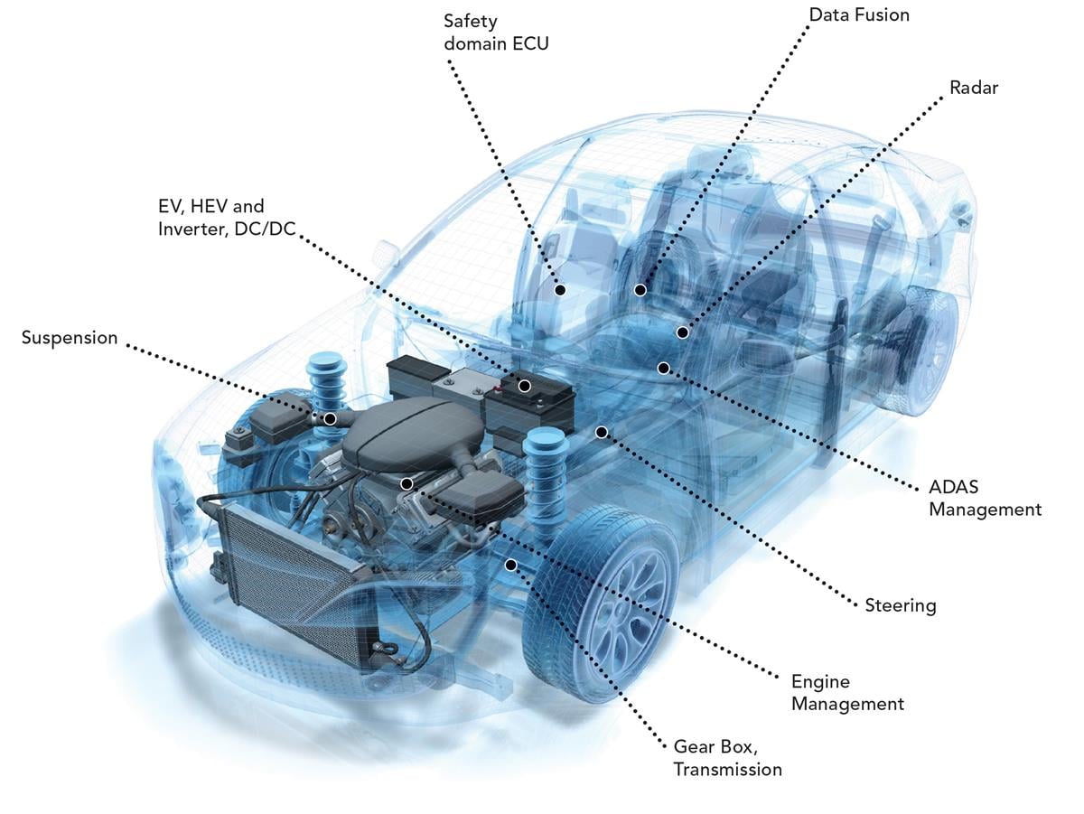
Applications Infographic

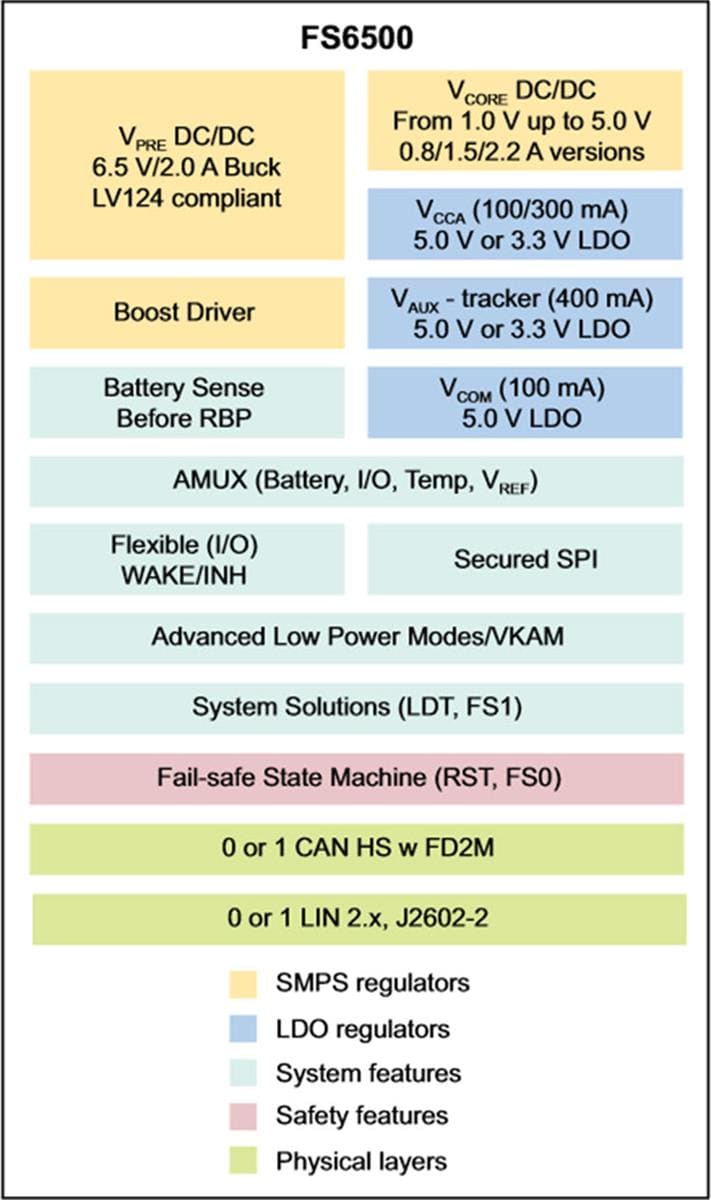
Simple Block Diagram


